New research focusing on quantum well thickness in cyan green LEDs pave way for a better understanding of improving drop behaviour and bandwidth of LEDs.
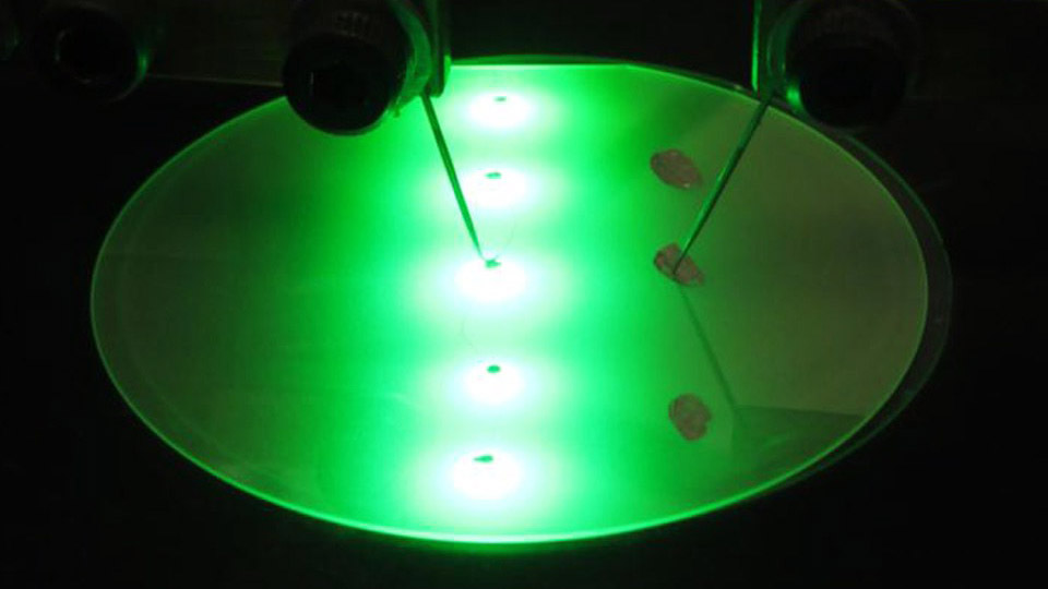
For the past few years, there has been an improved focus on the impact of quantum well thickness in indium gallium nitride (InGaN)/GaN green LEDs on competence droop. Droop is the decrease of emission effectiveness with rising injection current in InGaN/GaN multiple quantum well (MQW) LEDs that can critically limit their use like high-brightness lighting sources.
Quantum wells are thin layered semiconductor formations that derive majority of its properties from the quantum confinement of charge carriers in thin layers of a semiconductor ‘well’ matter squeeze in between an additional semiconductor barrier layers.
Such physical effects may as well be subjugated in real devices and, therefore, are the focus of a lot of research plans. When the quantum well is extremely thin, the boost of InGaN well layer thickness improves the polarization effect, making competence droop more serious. Relatively, increase in quantum well thickness considerably lessens droop.
Researchers from the National Central University in Taiwan, University of California Santa Barbara, and National Cheng Kung University in Taiwan augmented the modulation bandwidth of InGaN LEDs and, it was found that decreasing barrier thickness in the multiple quantum well active light-emitting areas improved bandwidth. The researchers claim record 3dB electrical-to-optical bandwidth values of almost 1GHz, as compared to other high-speed LEDs that administer less than 0.5GHz.
Researchers set out with an objective of increasing data rates for plastic optical fiber (POF) and visible-light communications with no equivalent increase in light-source price. Research involved evaluating devices with standard 17nm and thin 5nm barriers using LEDs appropriate for POF apps.
Team pointed out that there are two distinctions in the active MQWs of the design. Firstly, it is the immense decrease in thickness of the GaN barrier layer in the tool structure from 17nm to 5nm. Thinning down the layer facilitated entire thickness of the active layer to decrease from 97nm to 37nm, enhancing the modulation speed of the device, radiative recombination rate and injected carrier density.
The device types were developed on patterned sapphire and the active area was just about 50μm in diameter, while the device dimensions were 0.75×0.86mm, which included contact pads on the sapphire substrate. By inserting the metal pads on insulating sapphire, resistor-capacitor (RC) setbacks are minimized, increasing bandwidth.
Furthermore, the researchers said that equivalent output power of the devices at that temperature reveals that the thin barrier design does not considerably boost the likelihood of carriers escaping under high junction temperatures. The necessary driving current and fabrication price of GaN laser diodes are higher than would be needed for LED-based solutions. At 110°C, the bandwidths at 60mA were 0.64GHz for the standard MQW LEDs and 0.71GHz for thin barriers, the researchers added.
BizLED Magazine